∑ 125∞C operation
∑ 1 µs transient response
∑ >3.5 million hours MTBF
∑ Typical efficiency 94% at 2 V/50 A
∑ No output filtering required
∑ BGA or J-Lead packages
Vicor Corporation
Tel: 800-735-6200 V∑I Chip Voltage Transformation Module V048K020T080 Rev. 1.2 Page 1 of 15
vicorpower.com
PRELIMIN
ARY
Product Description
The V048K020T080 V
∑
I Chip Voltage Transformation
Module (VTM) breaks records for speed, density and
efficiency to meet the demands of advanced DSP,
FPGA, ASIC, processor cores and microprocessor
applications at the point of load (POL) while providing
isolation from input to output. It achieves a response
time of less than 1 µs and delivers up to 80 A in a
volume of less than 0.25 in
3
while providing low output
voltages with unprecedented efficiency. It may be
paralleled to deliver hundreds of amps at an output
voltage settable from 1.1 to 2.3 Vdc.
The VTM V048K020T080's nominal output voltage is
2 Vdc from a 48 Vdc input factorized bus, V
f
, and is
controllable from 1.1 to 2.3 Vdc at no load, and from
1.1 to 2.2 Vdc at full load, over a V
f
input range of 26
to 55 Vdc. It can be operated either open- or closed-loop
depending on the output regulation needs of the
application. Operating open-loop, the output voltage
tracks its V
f
input voltage with a transformation ratio,
K = 1/24, and an output resistance, R
OUT
= 1.3 milliohm, to
enable applications requiring a programmable low
output voltage at high current and high efficiency.
Closing the loop back to an input Pre-Regulation
Module (PRM) or DC-DC converter can compensate
for R
OUT
.
The 2 V VTM achieves break-through current density of
320 A/in
3
in a V
∑
I Chip package compatible with
standard pick-and-place and surface mount assembly
processes. The V
∑
I Chip BGA package supports in-board
mounting with a low profile of 0.16" (4 mm) over the
board. A J-lead package option supports on-board
surface mounting with a profile of only 0.25" (6 mm)
over the board. The VTM's fast dynamic response and
low noise eliminate the need for bulk capacitance at the
load, substantially increasing the POL density while
improving reliability and decreasing cost.
Absolute Maximum Ratings
Parameter
Values
Unit
Notes
+In to -In
-1.0 to 60.0
Vdc
+In to -In
100
Vdc
For 100 ms
PC to -In
-0.3 to 7.0
Vdc
TM to -In
-0.3 to 7.0
Vdc
VC to -In
-0.3 to 19.0
Vdc
+Out to -Out
-0.1 to 4.0
Vdc
Isolation voltage
2,250
Vdc
Input to Output
Operating junction temperature
-40 to 125
∞C
See Note
Output current
80
A
Continuous
Peak output current
120
A
For 1 ms
Case temperature during reflow
208
∞C
Storage temperature
-40 to 150
∞C
Output power
174
W
Continuous
Peak output power
261
W
For 1 ms
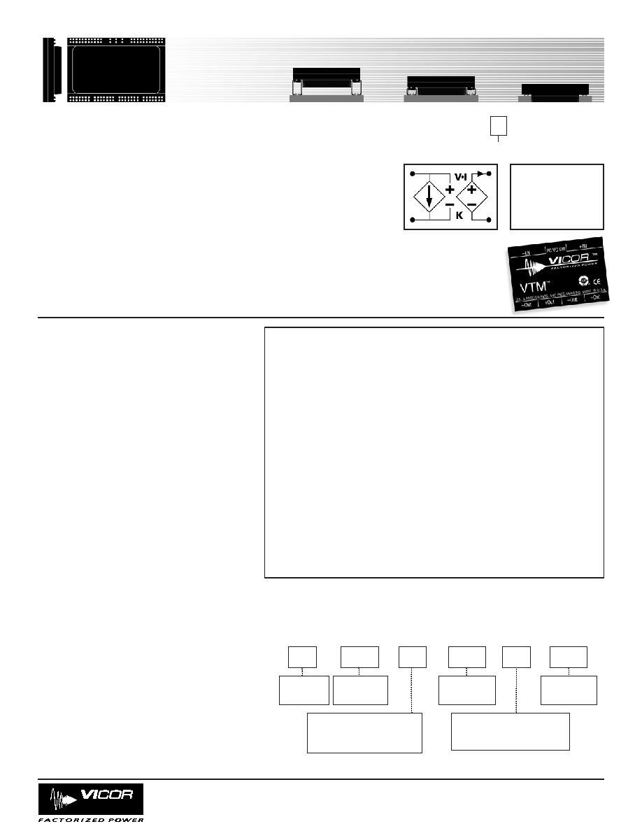
V∑I Chip
TM
≠ VTM
Voltage Transformation Module
∑ 48 V to 2 V V∑I Chip Converter
∑ 80 A (120 A for 1 ms)
∑ High density ≠ 320 A/in
3
∑ Small footprint ≠ 75 A/in
2
∑ Low weight ≠ 0.5 oz (14 g)
∑ Pick & Place / SMD
V048K020T080
V
f
= 26 - 55 V
V
OUT
= 1.1 - 2.3 V
I
OUT
= 80 A
K = 1/24
R
OUT
= 1.5 m
max
Actual size
©
VTM
Note:
The referenced junction is defined as the semiconductor having the highest temperature.
This temperature is monitored by the temperature monitor (TM) signal and by a shutdown comparator.
K indicates BGA configuration. For other
mounting options see Part Numbering below.
Output Current
Designator
(=I
OUT
)
V
048
K
020
T
080
Voltage
Transformation
Module
Input Voltage
Designator
Product Grade Temperatures (∞C)
Grade
Storage
Operating
T
-40 to150
-40 to125
Configuration Options
F = On-board (Fig.15)
K = In-board (Fig.14)
Output Voltage
Designator
(=V
OUT
x10)
Part Numbering
Vicor Corporation
Tel: 800-735-6200 V∑I Chip Voltage Transformation Module V048K020T080 Rev. 1.2 Page 2 of 15
vicorpower.com
PRELIMIN
ARY
Specifications
Parameter
Min
Typ
Max
Unit
Note
Input voltage range
26
48
55
Vdc
Operable down to zero V with external bias voltage
Input dV/dt
1
V/µs
Input overvoltage turn-on
56.0
Vdc
Input overvoltage turn-off
59.5
Vdc
Input current
3.7
Adc
Input reflected ripple current
170
mA p-p
Using test circuit in Fig.16; See Fig.1
No load power dissipation
2.50
3.15
W
Internal input capacitance
4
µF
Internal input inductance
20
nH
INPUT (Conditions are at 48 Vin, full load, and 25∞C ambient unless otherwise specified)
Parameter
Min
Typ
Max
Unit
Note
Rated DC current
0
80
Adc
Peak repetitive current
120
A
Max pulse width 1ms, max duty cycle 10%,
baseline power 50%
DC current limit
82
99
112
Adc
Current share accuracy
5
10
%
See Parallel Operation on page 10
Efficiency
Half load
94.0
94.2
%
See Fig.3, 2 Vout
Full load
93.0
93.2
%
See Fig.3, 2 Vout
Internal output inductance
0.8
nH
Internal output capacitance
306
µF
Effective value
Load capacitance
56,300
µF
Output overvoltage setpoint
2.33
Vdc
Output ripple voltage
No external bypass
53
65
mV
See Figs.2 and 5
100 µF bypass capacitor
2
mV
See Fig.6
Effective switching frequency
2.52
2.65
2.78
MHz
Fixed, 1.33 MHz per phase
Line regulation
K
0.0413
1/24
0.0421
V
OUT
= K∑V
IN
at no load
Load regulation
R
OUT
1.3
1.5
m
See Fig.19
Transient response
Voltage overshoot
20
mV
80 A load step with 100 µF C
IN;
See Figs.7 and 8
Response time
200
ns
See Figs.7 and 8
Recovery time
1
µs
See Figs.7 and 8
OUTPUT (Conditions are at 48 Vin, full load, and 25∞C ambient unless otherwise specified)

Vicor Corporation
Tel: 800-735-6200 V∑I Chip Voltage Transformation Module V048K020T080 Rev. 1.2 Page 3 of 15
vicorpower.com
Specifications
Figure 1-- Input reflected ripple current at full load and 48 Vin
Efficiency vs. Output Current
85
86
87
88
89
90
91
92
93
94
95
0
10
20
30
40
50
60
70
80
Output Current (A)
1.2 V
1.5 V
1.8 V
2.0 V
Efficiency (%)
Figure 3-- Efficiency vs. output current and output voltage
Power Dissipation vs. Output Current
0
2
4
6
8
10
12
14
0
10
20
30
40
50
60
70
80
Output Current (A)
1.2V
1.5V
1.8V
2.0V
Power Disipation (W)
Figure 4--Power dissipation as a function of output current and
output voltage
WAVEFORMS
Figure 6--Output voltage ripple at full load and 2 Vout with
100 µF ceramic external bypass capacitance and 20 nH
distribution inductance.
Figure 5-- Output voltage ripple at full load and 2 Vout;
without any external bypass capacitor.
Output Ripple vs Load
0
10
20
30
40
50
60
0
10
20
30
40
50
60
70
80
Output Currrent (A)
Output Ripple (mV)
Figure 2-- Output voltage ripple vs. output current at 2 Vout
with no POL bypass capacitance.
Vicor Corporation
Tel: 800-735-6200 V∑I Chip Voltage Transformation Module V048K020T080 Rev. 1.2 Page 4 of 15
vicorpower.com
PRELIMINARY
Parameter
Min
Typ
Max
Unit
Note
Primary Control (PC)
DC voltage
4.8
5.0
5.2
Vdc
Module disable voltage
2.4
2.5
Vdc
Module enable voltage
2.5
2.6
Vdc
Current limit
2.4
2.5
2.9
mA
Source only
Disable delay time
4
10
µs
PC low to Vout low
Temperature Monitor (TM)
27∞C setting
3.00
Vdc
Operating junction temperature
Temperature coefficient
10
mV/∞C
Full range accuracy
±5
∞C
Operating junction temperature
Current limit
100
µA
Source only
VTM Control (VC)
External boost voltage
12.0
14.0
19.0
Vdc
Required for VTM start up without PRM
External boost duration
10
ms
Vin must be >26 V for VTM to remain operating
without boost voltage.
Specifications, continued
Auxiliary Pins (Conditions are at 48 Vin, full load, and 25∞C ambient unless otherwise specified)
Parameter
Min
Typ
Max
Unit
Note
MTBF
MIL-HDBK-217F
3.5
Mhrs
25∞C, GB
Isolation specifications
Voltage
2,250
Vdc
Input to Output
Capacitance
2,500
pF
Input to Output
Resistance
10
M
Input to Output
Agency approvals (pending)
cTÐVus
UL/CSA 60950, EN 60950
CE Mark
Low voltage directive
Mechanical parameters
See mechanical drawing, Figs.10 and 12
Weight
0.5 / 14.0
oz / g
Dimensions(BGA version)
Length
1.26 / 32
in / mm
Width
0.85 / 21.5
in / mm
Height
0.23 / 5.9
in / mm
GENERAL
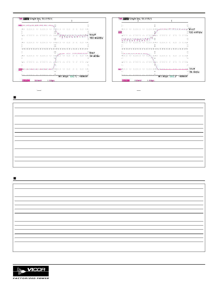
Figure 7-- 0-80 A step load change with 100 µF input
capacitance and no output capacitance.
Figure 8-- 80-0 A step load change with 100 µF input
capacitance and no output capacitance.

Vicor Corporation
Tel: 800-735-6200 V∑I Chip Voltage Transformation Module V048K020T080 Rev. 1.2 Page 5 of 15
vicorpower.com
PRELIMIN
ARY
Specifications, continued
V∑I CHIP STRESS DRIVEN PRODUCT QUALIFICATION PROCESS
Symbol
Parameter
Min
Typ
Max
Unit
Note
Over temperature shutdown
125
130
135
∞C
Junction temperature
Thermal capacity
0.61
Ws/∞C
R
JC
Junction-to-case thermal impedance
1.1
∞C/W
R
JB
Junction-to-BGA thermal impedance
2.1
∞C/W
R
JA
Junction-to-ambient
1
6.5
∞C/W
R
JA
Junction-to-ambient
2
5.0
∞C/W
THERMAL
Notes
1. V048K020T080 surface mounted in-board to a 2" x 2" FR4 board, 4 layers 2 oz Cu, 300 LFM.
2. V048K020T080 with a 0.25"H heatsink surface mounted on FR4 board, 300 LFM.
Test
Standard
Environment
High Temperature Operational Life (HTOL)
JESD22-A-108-B
125∞C, Vmax, 1,008 hrs
Temperature cycling
JESD22-A-104B
-55∞C to 125∞C, 1,000 cycles
High temperature storage
JESD22-A-103A
150∞C, 1,000 hrs
Moisture resistance
JESD22-A113-B
Moisture sensitivity Level 5
Temperature Humidity Bias Testing (THB)
EIA/JESD22-A-101-B
85∞C, 85% RH, Vmax, 1,008 hrs
Pressure cooker testing (Autoclave)
JESD22-A-102-C
121∞C, 100% RH, 15 PSIG, 96 hrs
Highly Accelerated Stress Testing (HAST)
JESD22-A-110B
130∞C, 85% RH, Vmax, 96 hrs
Solvent resistance/marking permanency
JESD22-B-107-A
Solvents A, B & C as defined
Mechanical vibration
JESD22-B-103-A
20g peak, 20-2,000 Hz, test in X, Y & Z directions
Mechanical shock
JESD22-B-104-A
1,500g peak 0.5 ms pulse duration, 5 pulses in 6 directions
Electro static discharge testing ≠ human body model
EIA/JESD22-A114-A
Meets or exceeds 2,000 Volts
Electro static discharge testing ≠ machine model
EIA/JESD22-A115-A
Meets or exceeds 200 Volts
Highly Accelerated Life Testing (HALT)
Per Vicor Internal
Operation limits verified, destruct margin determined
Test Specification*
Dynamic cycling
Per Vicor internal
Constant line, 0-100% load, -20∞C to 125∞C
test specification*
* For details of the test protocols see Vicor's website.
Test
Standard
Environment
BGA solder fatigue evaluation
IPC-9701
Cycle condition: TC3 (-40 to +125∞C)
IPC-SM-785
Test duration: NTC-B (500 failure free cycles)
Solder ball shear test
IPC-9701
Failure through bulk solder or copper pad lift-off
V∑I CHIP BALL GRID ARRAY INTERCONNECT QUALIFICATION
Vicor Corporation
Tel: 800-735-6200 V∑I Chip Voltage Transformation Module V048K020T080 Rev. 1.2 Page 6 of 15
vicorpower.com
PRELIMINARY
PRELIMIN
ARY
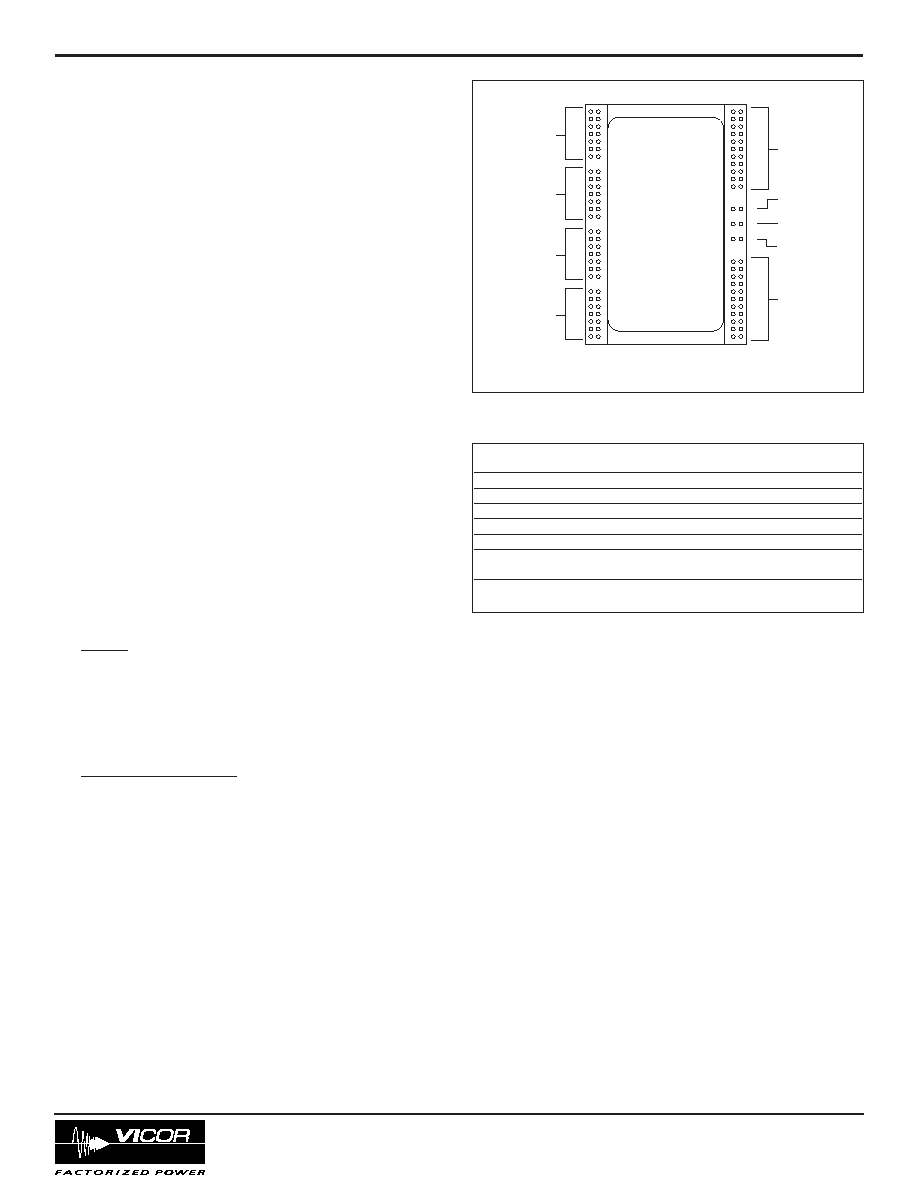
Pin/Control Functions
+IN/-IN DC VOLTAGE PORTS
The VTM input should not exceed the high end of the range
specified. Be aware of this limit in applications where the VTM
is being driven above its nominal output voltage. A 14 V source
must be applied to the VC pin and voltage must be present at
the +In and -In ports in order for the VTM to process power. If
the input voltage exceeds the over voltage lock-out, the VTM
will shutdown. The VTM does not have internal input reverse
polarity protection. Adding a properly sized diode in series with
the positive input or a fused reverse-shunt diode will provide
reverse polarity protection.
VC ≠ VTM Control
The VC port is multiplexed. It receives the initial Vcc voltage
from an upstream PRM, synchronizing the output rise of the
VTM with the output rise of the PRM. Additionally, the VC
port provides feedback to the PRM to compensate for the VTM
output resistance. In typical applications using VTMs powered
from PRMs, the PRM's VC port should be connected to the
VTM VC port.
In applications where a VTM is being used without a PRM,
14 V must be supplied to the VC port for approximately 10 ms in
order for the VTM to startup. The VTM can be operated at
input voltages below 26 V as long as the VC voltage is applied.
PC ≠ Primary Control
The Primary Control (PC) pin is a multifunction pin for
controlling the VTM as follows:
Disable ≠ If the PC is left floating, the VTM output
is enabled. To disable the output, the PC pin must be pulled
lower than 2.4 V, referenced to -In. Optocouplers, open
collector transistors or relays can be used to control the PC
pin. Once disabled, 14 V must be re-applied to the VC pin
in order to restart the VTM
Primary Auxiliary Supply ≠ The PC port can source up to
2.4 mA at 5 Vdc.
TM ≠ Temperature Monitor
The Temperature Monitor (TM) provides a linear output
proportional to the internal temperature of the VTM. At 300∫K
(+27∫C) the TM output is 3.0 V referenced to -In and varies
10 mV/∫C. TM accuracy is +/-5∫C. This feature is useful for
validating the thermal design of the system as well as
monitoring the VTM temperature in the final application.
+OUT/-OUT DC Voltage Output Ports
The output (+OUT) and output return (-OUT) are through two
sets of contact locations. The respective +OUT and ≠OUT
groups must be connected in parallel with as low an
interconnect resistance as possible. Within the specified input
voltage range, the Level 1 DC behavioral model shown in
Figure 19 defines the output voltage of the VTM. The current
source capability of the VTM is shown in the specification table.
To take full advantage of the VTM, the user should note the
low output impedance of the device. The low output impedance
provides fast transient response without the need for bulk POL
capacitance. Limited-life electrolytic capacitors required with
conventional converters can be reduced or even eliminated,
saving cost and valuable board real estate.
-In
Primary
Control
VTM Control
Temp.
Monitor
+In
-Out
+Out
-Out
+Out
Bottom View
A
B
C
D
E
F
G
H
J
K
L
M
N
P
R
T
U
V
W
Y
AA
AB
AC
AD
AE
AF
AG
AH
AJ
AK
AL
4 3 2 1
A
B
C
D
E
F
G
H
J
K
L
M
N
P
R
T
U
V
W
Y
AA
AB
AC
AD
AE
AF
AG
AH
AJ
AK
AL
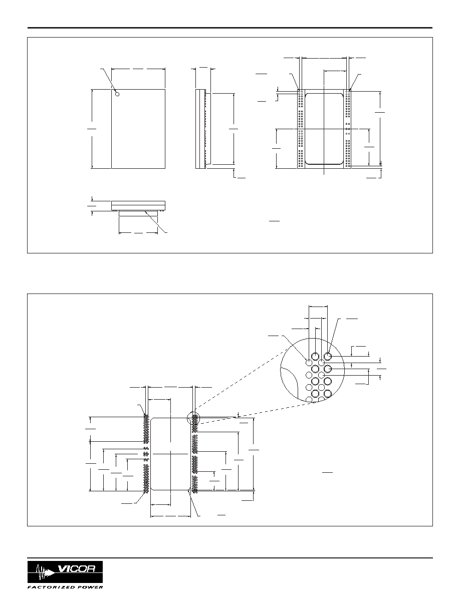
Figure 9--VTM BGA configuration
Signal BGA
Name
Designation
+In
A1-L1, A2-L2
≠In
AA1-AL1, AA2-AL2
TM
P1, P2
VC
T1, T2
PC
V1, V2
+Out
A3-G3, A4-G4,
U3-AC3, U4-AC4
≠Out
J3-R3, J4-R4,
AE3-AL3, AE4-AL4
Vicor Corporation
Tel: 800-735-6200 V∑I Chip Voltage Transformation Module V048K020T080 Rev. 1.2 Page 7 of 15
vicorpower.com
NOTES:
1- DIMENSIONS ARE .
2- UNLESS OTHERWISE SPECIFIED, TOLERANCES ARE:
.X/[.XX] = +/-0.25/[.01]; .XX/[.XXX] = +/-0.13/[.005]
3- PRODUCT MARKING ON TOP SURFACE
inch
mm
30,00
1.181
1,00
0.039
15,00
0.591
18,00
0.709
1,00
0.039
9,00
0.354
1,00
0.039
1,00
0.039
INPUT
OUTPUT
L
L
C
C
BOTTOM VIEW
SOLDER BALL #A1
SEATING PLANE
TOP VIEW (COMPONENT SIDE)
OUTPUT
INPUT
SOLDER BALL
#A1 INDICATOR
TYP
3,9
0.15
15,6
0.62
21,5
0.85
32,0
1.26
1,6
0.06
28,8
1.13
5,9
0.23
16,0
0.63
(106) X ÿ
0.51
0.020
SOLDER BALL
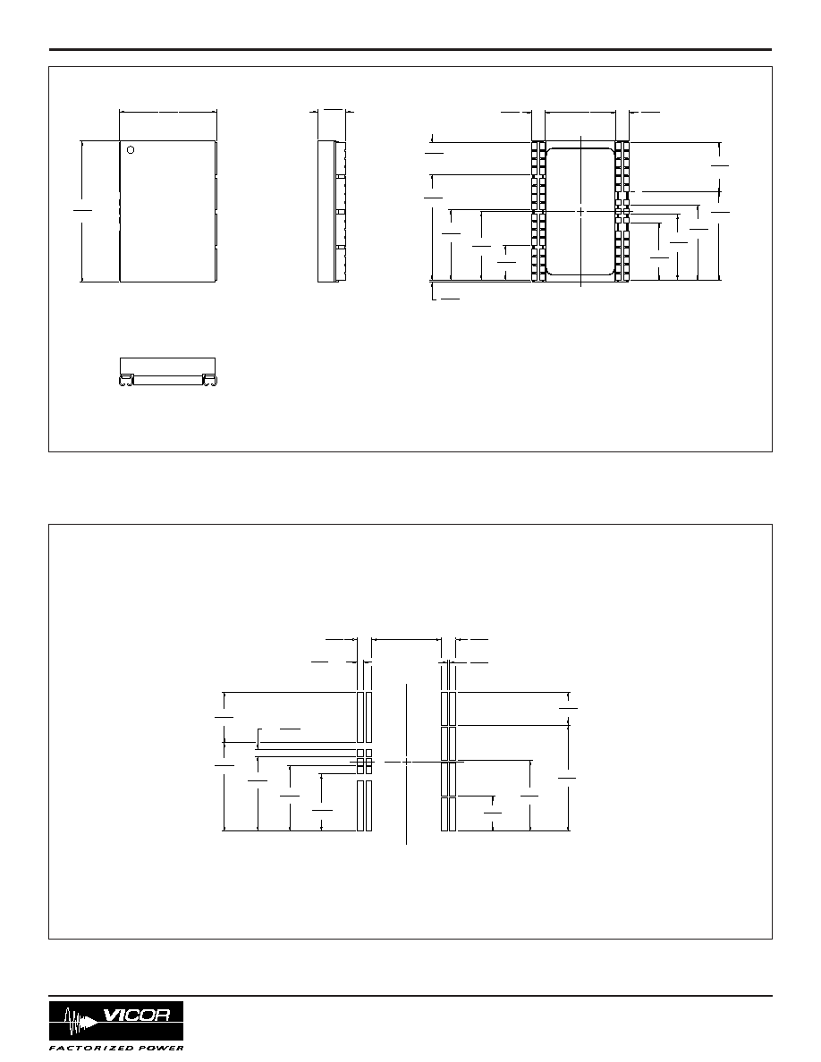
Mechanical Drawings
PRELIMINARY
Figure 10-- V T M BGA mechanical outline; In-board mounting
NOTES:
1- DIMENSIONS ARE .
2- UNLESS OTHERWISE SPECIFIED, TOLERANCES ARE:
.X/[.XX] = +/-0.25/[.01]; .XX/[.XXX] = +/-0.13/[.005]
inch
mm
15,00
0.591
17,00
0.669
20,00
0.787
13,00
0.512
16,00
0.630
24,00
0.945
8,00
0.315
16,16
0.636
8,08
0.318
18,00
0.709
1,00
0.039
9,00
0.354
0,37
0.015
29,26
1.152
(2) X
0.394
(4) X
0.236
1,00
0.039
PCB CUTOUT
+IN
+OUT1
-OUT1
+OUT2
-OUT2
-IN
VC
TM
PC
SOLDER PAD #A1
RECOMMENDED LAND AND VIA PATTERN
(COMPONENT SIDE SHOWN)
SOLDER MASK
DEFINED PAD
1,6
0.06
0,51
0.020
1,00
0.039
1,50
0.059
0,50
0.020
1,00
0.039
0,50
0.020
1,00
0.039
SOLDER MASK
DEFINED PADS
CONNECT TO
INNER LAYERS
0,51
0.020
0,53
0.021
10,00
6,00
(106) X ¯
(4) X R
( ¯ )
( )
¯ PLATED VIA
( )
31
1
Figure 11-- VTM BGA PCB land/VIA layout information; In-board mounting
IN-BOARD MOUNTING
BGA surface mounting requires a
cutout in the PCB in which to recess the V∑I Chip
Vicor Corporation
Tel: 800-735-6200 V∑I Chip Voltage Transformation Module V048K020T080 Rev. 1.2 Page 8 of 15
vicorpower.com
NOTES:
1- DIMENSIONS ARE mm/[INCH].
2- UNLESS OTHERWISE SPECIFIED, TOLERANCES ARE:
.X/[.XX] = +/-0.25/[.01]; .XX/[.XXX] = +/-0.13/[.005]
3- PRODUCT MARKING ON TOP SURFACE
C
CL
L
16,00
0.630
24,00
0.945
0,45
0.018
8,00
0.315
14,94
0.588
16,94
0.667
20,00
0.787
12,94
0.509
15,99
0.630
3,01
0.118
3,01
0.118
7,10
0.280
(4) PL.
11,10
0.437
(2) PL.
6,1
0.24
32,0
22,0
0.87
BOTTOM VIEW
OUTPUT
INPUT
OUTPUT
INPUT
TOP VIEW (COMPONENT SIDE)
1.26
15,55
0.612
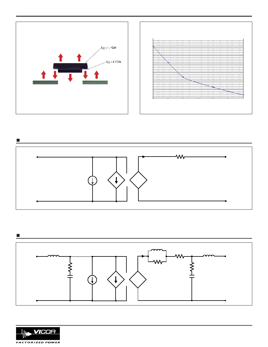
Mechanical Drawings
PRELIMINARY
Figure 12-- V T M J-lead mechanical outline; On-board mounting
NOTES:
1- DIMENSIONS ARE mm/[INCH].
2- UNLESS OTHERWISE SPECIFIED, TOLERANCES ARE:
.X/[.XX] = +/-0.25/[.01]; .XX/[.XXX] = +/-0.13/[.005]
14,94
0.588
16,94
0.667
20,00
0.787
12,94
0.509
16,00
0.630
24,00
0.945
8,00
0.315
15,74
0.620
3,26
0.128
3,26
0.128
0,51
0.020
1,38
0.054
11,48
0.452
1,60
0.063
7,48
0.295
(COMPONENT SIDE SHOWN)
RECOMMENDED LAND PATTERN
-IN
PC
VC
TM
+IN
+OUT1
-OUT1
+OUT2
-OUT2
(4) X
(6) X
(2) X
(2) X
(2) X
(2) X
TYP
TYP
(8) X
(2) X
(2) X
(2) X
Figure 13-- VTM J-lead PCB land layout information; On-board mounting

Vicor Corporation
Tel: 800-735-6200 V∑I Chip Voltage Transformation Module V048K020T080 Rev. 1.2 Page 9 of 15
vicorpower.com
PRELIMIN
ARY
IN≠BOARD MOUNT
(V∑I Chip recessed into PCB)
21.5
0.85
32.0
1.26
4.0
0.16
CONFIGURATION OPTIONS
CONFIGURATION
IN-BOARD* ON-BOARD* IN-BOARD WITH 0.25" ON-BOARD WITH 0.25"
(Fig. 14) (Fig. 15) HEATSINK HEATSINK
Effective Current Density
467 A/in
3
292 A/in
3
182 A/in
3
146 A/in
3
Junction-Board
2.1 ∞C/W
2.4 ∞C/W
2.1 ∞C/W
2.4 ∞C/W
Thermal Resistance
Junction-Case
1.1 ∞C/W
1.1 ∞C/W
N/A
N/A
Thermal Resistance
Junction-Ambient
6.5 ∞C/W
6.8 ∞C/W
5.0 ∞C/W
5.0 ∞C/W
Thermal Resistance 300LFM
*Surface mounted to a 2" x 2" FR4 board, 4 layers 2 oz Cu
Figure 14--In-board mounting ≠ package K
ON≠BOARD MOUNT
22.0
0.87
32.0
1.26
6.3
0.25
Figure 15--On-board mounting ≠ package F
mm
in
mm
in

Vicor Corporation
Tel: 800-735-6200 V∑I Chip Voltage Transformation Module V048K020T080 Rev. 1.2 Page 10 of 15
vicorpower.com
PRELIMINARY
Configuration Options (Cont.)
Figure 16--VTM test circuit
F1
Temperature Monitor
Load
+
≠
7 A
Fuse
C1
100
µ
F
Al electrolytic
+
≠
Input reflected ripple
measurement point
C2
0.47
µ
F
ceramic
+
≠
14 V
-In
PC
VC
TM
+In
-Out
+Out
VTM
+Out
-Out
K
Ro
Application Note
Parallel Operation
In applications requiring higher current or redundancy, VTMs
can be operated in parallel without adding control circuitry or
signal lines. To maximize current sharing accuracy, it is imperative
that the source and load impedance on each VTM in a parallel
array be equal. If VTMs are being fed by an upstream PRM, the
VC nodes of all VTMs must be connectd to the PRM VC.
To achieve matched impedances, dedicated power planes
within the PC board should be used for the output and output
return paths to the array of paralleled VTMs. This technique is
preferable to using traces of varying size and length.
The VTM power train and control architecture allow bi-directional
power transfer when the VTM is operating within its specified
ranges. Bi-directional power processing improves transient
response in the event of an output load dump. The VTM may
operate in reverse, returning output power back to the input
source. It does so efficiently.
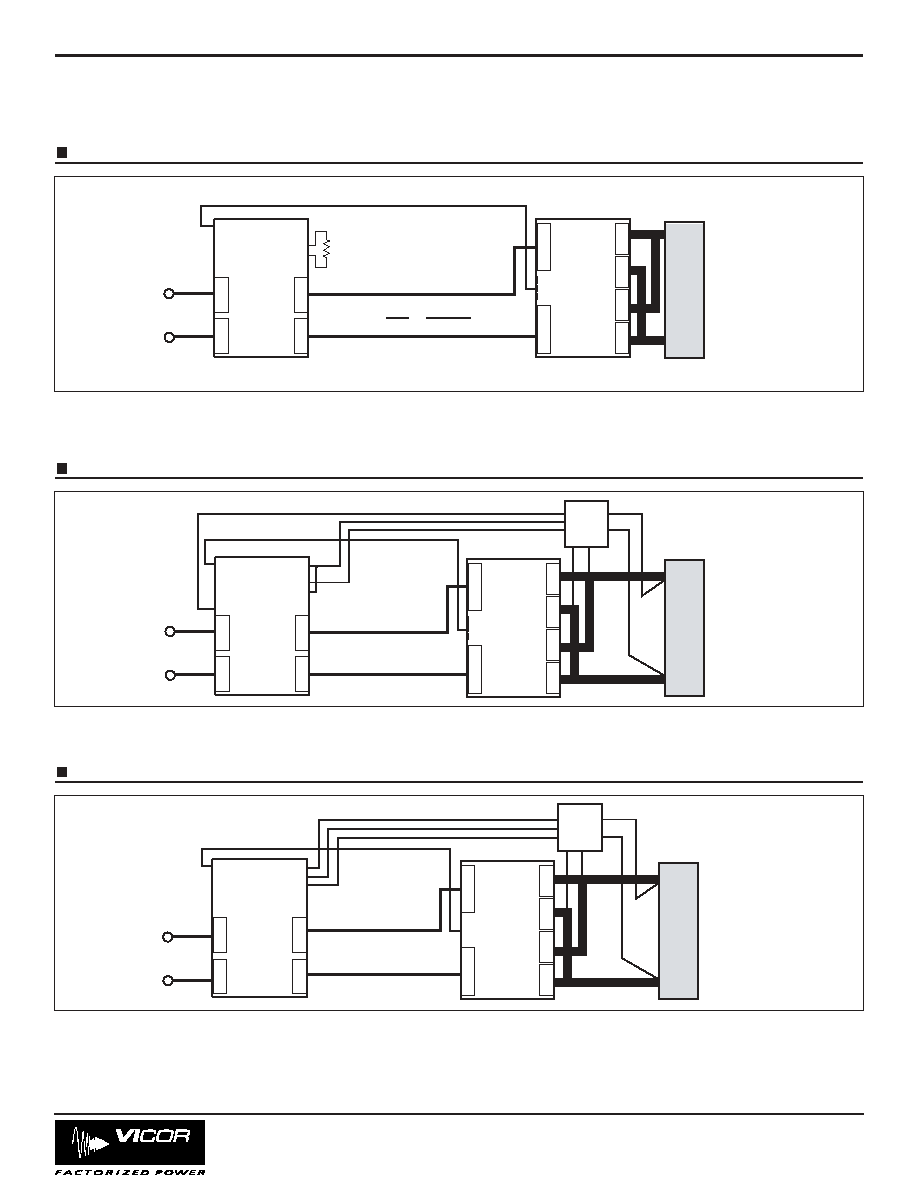
Thermal Management
The high efficiency of the VTM results in low power
dissipation minimizing temperature rise, even at full output
current. The heat generated within the internal semiconductor
junctions is coupled through very low thermal resistances, R
JC
and R
JB
(see Figure 17), to the PC board allowing flexible
thermal management.
CASE 1 Convection via optional heatsink to air
In an environment with forced convection over the surface
of a PCB with 0.4" of headroom, a VTM with a 0.25 heat sink
offers a simple thermal management option. The total
Junction toAmbient thermal resistance of a surface mounted
V048K020T080 with a heat sink attached is 4.8 ∫C/W in
300 LFMairflow, (see Figure 18).
At 2 Vout and full rated current (80A), the VTM dissipates
approximately 12 W per Figure 4. This results in a temperature
rise of approximately 56 ∫C, allowing operation in an air
temperature of 69 ∫C without exceeding the 125 ∫C max
junction temperature.
CASE 2 Conduction via the PC board to air
The low Junction to BGA thermal resistance allows the use
of the PC board as a means of removing heat from the VTM.
Convection from the PC board to ambient, or conduction to a
cold plate, enable flexible thermal management options.
With a VTM mounted on a 2.0 in
2
area of a multi-layer PC
board with appropriate power planes resulting in 8 oz of
effective copper weight, the Junction-to-BGA thermal
resistance, R
JA
, is 6.5 ∫C/W in 300 LFM of air. With a
maximum junction temperature of 125 ∫C and 12 W of
dissipation at full current of 80 A, the resulting temperature
rise of 76 ∫C allows the VTM to operate at full rated current
up to a 49 ∫C ambient temperature. See thermal resistances
on page 9 for additional details on this thermal management option.
Adding low-profile heat sinks to the PC board can lower the
thermal resistance of the PC board surrounding the VTM.
Additional cooling may be added by coupling a cold plate to
the PC board with low thermal resistance stand offs.
CASE 3 Combined direct convection to the air and conduction
to the PC board.
A combination of cooling techniques that utilize the power
planes and dissipation to the air will also reduce the total
thermal impedance. This is the most effective cooling
method. To estimate the total effect of the combination, treat
each cooling branch as one leg of a parallel resistor network.
Notes:
C3 should be placed close to the load
C3
100 µF
15 m
I
Q
52 mA
Vicor Corporation
Tel: 800-735-6200 V∑I Chip Voltage Transformation Module V048K020T080 Rev. 1.2 Page 11 of 15
vicorpower.com
Figure 18--Junction-to-ambient thermal resistance of VTM
with 0.25" Heat Sink.
VTM with 0.25'' heat sink
3
4
5
6
7
8
9
10
0
100
200
300
400
500
600
Airflow (LFM)
Tja
Application Note (continued)
PRELIMINARY
Figure 17--Thermal resistance
V∑I Chip VTM LEVEL 1 DC BEHAVIORAL MODEL for 48V to 2V, 80A
Figure 19--This model characterizes the DC operation of the V∑I Chip VTM, including the converter transfer function
and its losses. The model enables estimates or simulations of output voltage as a function of input voltage and output load, as
well as total converter power dissipation or heat generation.
©
+
≠
+
≠
V
OUT
C
OUT
V
IN
V
∑
I
K
+
≠
+
≠
C
IN
I
OUT
R
OUT
V∑I Chip VTM LEVEL 2 TRANSIENT BEHAVIORAL MODEL for 48V to 2V, 80A
Figure 20--This model characterizes the AC operation of the V∑I Chip VTM including response to output load or input voltage
transients or steady state modulations. The model enables estimates or simulations of input and output voltages under transient
conditions, including response to a stepped load with or without external filtering elements.
©
1.3 m
1/24 ∑ Vin
1/24 ∑ Iout
I
Q
52 mA
+
≠
+
-
V
OUT
V
IN
V
∑
I
K
+
≠
+
≠
I
OUT
R
OUT
1/24 ∑ Iout
1/24 ∑ Vin
1.3 m
L
I
N
= 20 nH
RC
I
N
1.3 m
0.12 nH
0.6 m
RC
OUT
65 µ
306 µF
L
OUT
= 0.8 nH
4 µF
Vicor Corporation
Tel: 800-735-6200 V∑I Chip Voltage Transformation Module V048K020T080 Rev. 1.2 Page 12 of 15
vicorpower.com
Application Note (continued)
Figure 21 -- The PRM controls the factorized bus voltage, Vf, in proportion to output current to compensate for the output resistance,
Ro, of the VTM. The VTM output voltage is typically within 1% of the desired load voltage (V
L
) over all line and load conditions.
-In
PC
VC
TM
+In
-Out
+Out
VTM
+Out
-Out
K
Ro
+Out
≠Out
+In
≠In
VC
PC
TM
IL
VH
PR
NC
SG
SC
PRM-AL
OS
NC
CD
L
O
A
D
Factorized
Power Bus
Vin
Vo = V
L ±
1.0%
(Io∑Ro)
K
Rs
V
f
=
V
L
+
K
FPA Adaptive Loop
Figure 22 -- An external error amplifier or Point-of-Load IC (POLIC) senses the load voltage and controls the PRM output ≠ the
factorized bus ≠ as a function of output current, compensating for the output resistance of the VTM and for distribution resistance.
+Out
≠Out
+In
≠In
VC
PC
TM
IL
VH
PR
NC
SG
SC
PRM-AL
OS
NC
CD
-In
PC
VC
TM
+In
-Out
+Out
VTM
+Out
-Out
K
Ro
Remote
Loop
Control
V
f
= f (Vs)
L
O
A
D
Vin
Factorized
Power Bus
Vo = V
L ±
0.4%
+S
≠S
FPA Non-isolated Remote Loop
In figures 21 ≠ 24;
K = VTM Transformation Ratio
Vf = PRM Output (Factorized Bus Voltage)
Ro = VTM Output Resistance
Vo = VTM Output
V
L
= Desired Load Voltage
FPA Isolated Remote Loop
VC
PC
TM
IL
VS
PR
NC
FG
FB
PRM-IF
NC
NC
NC
+Out
≠Out
+In
≠In
-In
PC
VC
TM
+In
-Out
+Out
VTM
+Out
-Out
K
Ro
V
f
= f (Vs)
Factorized
Power Bus
Vin
Remote
Loop
Control
L
O
A
D
Vo = V
L ±
0.4%
+S
≠S
Figure 23--An external error amplifier or Point-of-Load IC (POLIC) senses the load voltage and controls the PRM output ≠ the
factorized bus ≠ as a function of output current, compensating for the output resistance of the VTM and for distribution
resistance. The factorized bus voltage (Vf) increases in proportion to load current. The remote feed back loop is isolated within
the PRM to support galvanic isolation and hipot compliance at the system level.
Vicor Corporation
Tel: 800-735-6200 V∑I Chip Voltage Transformation Module V048K020T080 Rev. 1.2 Page 13 of 15
vicorpower.com
Application Note (continued)
PRELIMINARY
V∑I Chip Soldering Recommendations
V∑I Chip modules are intended for reflow soldering processes.
The following information defines the processing conditions
required for successful attachment of a V∑I Chip to a PCB.
Failure to follow the recommendations provided can result in
aesthetic or functional failure of the module.
Storage
V∑I Chip modules are currently rated at MSL 5. Exposure to
ambient conditions for more than 72 hours requires a 24 hour
bake at 125∫C to remove moisture from the package.
Solder Paste Stencil Design
Solder paste is recommended for a number of reasons, including
overcoming minor solder sphere co-planarity issues as well as
simpler integration into overall SMD process.
63/37 SnPb, either no-clean or water-washable, solder paste
should be used. Pb-free development is underway.
The recommended stencil thickness is 6 mils. The apertures
should be 20 mils in diameter for the In-Board (BGA)
application and 0.9-0.9:1 for the On-Board (J-Leaded).
Pick & Place
In-Board (BGA) modules should be placed as accurately as
possible to minimize any skewing of the solder joint; a maximum
offset of 10 mils is allowable. On-Board (J-Leaded) modules
should be placed within ±5 mils.
To maintain placement position, the modules should not be
subjected to acceleration greater than 500 in/sec
2
prior to reflow.
Reflow
There are two temperatures critical to the reflow process; the
solder joint temperature and the module's case temperature. The
solder joint's temperature should reach at least 220∫C, with a
time above liquidus (183∫C) of ~30 seconds.
The module's case temperature must not exceed 208 ∫C at
anytime during reflow.
Because of the
T needed between the pin and the case, a forced-
air convection oven is preferred for reflow soldering. This
reflow method generally transfers heat from the PCB to the
solder joint. The module's large mass also reduces its
temperature rise. Care should be taken to prevent smaller
devices from excessive temperatures. Reflow of modules onto a
PCB using Air-Vac-type equipment is not recommended due to
the high temperature the module will experience.
Inspection
For the BGA-version, a visual examination of the post-reflow
solder joints should show relatively columnar solder joints with
no bridges. An inspection using x-ray equipment can be done,
but the module's materials may make imaging difficult.
The J-Lead version's solder joints should conform to IPC 12.2
∑ Properly Wetted Fillet must be evident
∑ Heel fillet height must exceed lead thickness plus solder thickness.
Removal and Rework
V∑I Chip modules can be removed from PCBs using special tools
such as those made by Air-Vac. These tools heat a very localized
region of the board with a hot gas while applying a tensile force
to the component (using vacuum). Prior to component heating
and removal, the entire board should be heated to 80-100∫C to
decrease the component heating time as well as local PCB
warping. If there are adjacent moisture-sensitive components, a
125∫C bake should be used prior to component removal to
prevent popcorning. V∑I Chip modules should not be expected to
survive a removal operation.
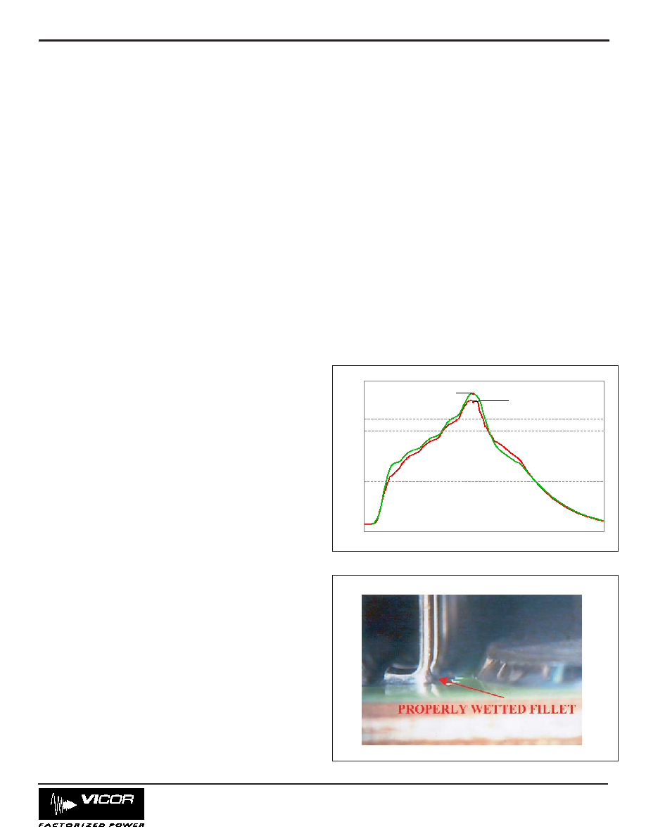
Case Temperature, 208∫C
Joint Temperature, 220∫C
239
165
91
16
degC
183
Soldering Time
Figure 25--Thermal profile diagram
Figure 26-- Properly reflowed V∑I Chip J-Lead.
©

Vicor Corporation
Tel: 800-735-6200 V∑I Chip Voltage Transformation Module V048K020T080 Rev. 1.2 Page 14 of 15
vicorpower.com
Application Note (continued)
PRELIMINARY
Input Impedance Recommendations
To take full advantage of the VTM's capabilities, the impedance
of the source (input source plus the PC board impedance) must be
low over a range from DC to 5 MHz. The input of the VTM
(factorized bus) should be locally bypassed with a 8 µF low Q
aluminum electrolytic capacitor. Additional input capacitance
may be added to improve transient performance or compensate
for high source impedance. The VTM has extremely wide
bandwidth so the source response to transients is usually the
limiting factor in overall output response of the VTM.
Anomalies in the response of the source will appear at the output
of the VTM, multiplied by its K factor of 1/24. The DC
resistance of the source should be kept as low as possible to
minimize voltage deviations on the input to the VTM. If the
VTM is going to be operating close to the high limit of its input
range, make sure input voltage deviations will not trigger the
over voltage shutdown.
Input Fuse Recommendations
V∑I Chips are not internally fused in order to provide flexibility
in power system configuration. However, input line fusing of
V∑I Chips must always be incorporated within the power system.
A fast acting fuse, such as NANO2 FUSE 451 Series 7 A 125 V,
is required to meet safety agency Conditions of Acceptability.
The input line fuse should be placed in series with the +IN port.
Warranty
Vicor products are guaranteed for two years from date of shipment against defects in material or workmanship when in normal use
and service. This warranty does not extend to products subjected to misuse, accident, or improper application or maintenance. Vicor
shall not be liable for collateral or consequential damage. This warranty is extended to the original purchaser only.
EXCEPT FOR THE FOREGOING EXPRESS WARRANTY, VICOR MAKES NO WARRANTY, EXPRESS OR IMPLIED, INCLUDING,
BUT NOT LIMITED TO, THE WARRANTY OF MERCHANTABILITY OR FITNESS FOR A PARTICULAR PURPOSE.
Vicor will repair or replace defective products in accordance with its own best judgement. For service under this warranty, the buyer
must contact Vicor to obtain a Return Material Authorization (RMA) number and shipping instructions. Products returned without
prior authorization will be returned to the buyer. The buyer will pay all charges incurred in returning the product to the factory. Vicor
will pay all reshipment charges if the product was defective within the terms of this warranty.
Information published by Vicor has been carefully checked and is believed to be accurate; however, no responsibility is assumed for
inaccuracies. Vicor reserves the right to make changes to any products without further notice to improve reliability, function, or
design. Vicor does not assume any liability arising out of the application or use of any product or circuit; neither does it convey any
license under its patent rights nor the rights of others. Vicor general policy does not recommend the use of its components in life
support applications wherein a failure or malfunction may directly threaten life or injury. Per Vicor Terms and Conditions of Sale, the
user of Vicor components in life support applications assumes all risks of such use and indemnifies Vicor against all damages.

Vicor Corporation
Tel: 800-735-6200 V∑I Chip Voltage Transformation Module V048K020T080 Rev. 1.2 Page 15 of 15
vicorpower.com 06/05
Vicor's comprehensive line of power solutions includes high density AC-DC
and DC-DC modules and accessory components, fully configurable AC-DC
and DC-DC power supplies, and complete custom power systems.
Information furnished by Vicor is believed to be accurate and reliable. However, no responsibility is
assumed by Vicor for its use. Vicor components are not designed to be used in applications, such as life
support systems, wherein a failure or malfunction could result in injury or death. All sales are subject to
Vicor's Terms and Conditions of Sale, which are available upon request.
Specifications are subject to change without notice.
Vicor Corporation
25 Frontage Road
Andover, MA, USA 01810
Tel: 800-735-6200
Fax: 978-475-6715
Email
Vicor Express: vicorexp@vicr.com
Technical Support: apps@vicr.com
Intellectual Property Notice
Vicor and its subsidiaries own Intellectual Property (issued U.S. and Foreign Patents and
pending patent applications) relating to the product described in this data sheet including;
∑ The electrical and thermal utility of the V∑I Chip package
∑ The design of the V∑I Chip package
∑ The Power Conversion Topology utilized in the V∑I Chip package
∑ The Control Architecture utilized in the V∑I Chip package
∑ The Factorized Power Architecture.
Purchase of this product conveys a license to use it. However, no responsibility is assumed
by Vicor for any infringement of patents or other rights of third parties which may result
from its use. Except for its use, no license is granted by implication or otherwise under any
patent or patent rights of Vicor or any of its subsidiaries.
Anybody wishing to use Vicor proprietary technologies must first obtain a license. Potential
users without a license are encouraged to first contact Vicor's Intellectual Property Department.